LAB2FAB
Workshop 2022
Shedding Light on Innovation
Virtual Seminars
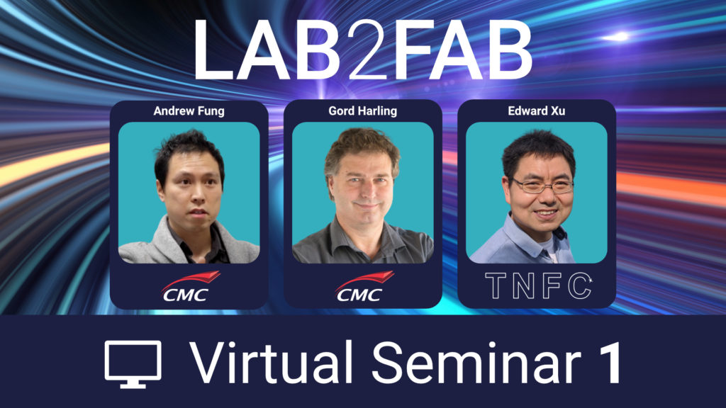
Virtual Seminar 1
Welcome – Opening remarks
Moderator:
CMC Microsystems
 Gord Harling
President and CEO, CMC Microsystems
Gordon Harling received a Bachelor’s degree in Applied Science from the University of Toronto and a Maîtrise en Ingénierie Physique from Polytechnique Montréal. He has worked in Research and Development at large companies such as Mitel, NovAtel, and DALSA. He has been a founder and CEO of several start-up companies including Goal Semiconductor, Elliptic Technologies, and Innotime Technologies. He joined CMC Microsystems in February 2018 as President and CEO.
Mohsen K. Akhlaghi
Director of Integrated Photonics, Photonic Inc.
Mohsen K. Akhlaghi received his B.Sc. and M.Sc. in electrical engineering from Tehran Polytechnic in 2000 and 2003. He held a variety of engineering and management positions in the industrial and consumer electronics sector. His Ph.D. from the University of Waterloo in 2012 was on detecting single photons using superconducting nanowires. After a postdoctoral at UBC, he joined Nanotech Security Corp. later acquired by Meta Materials Inc. Mohsen is currently Director of Integrated Photonics at Photonic Inc
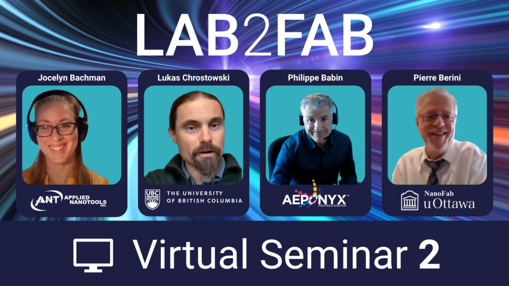
Virtual Seminar 2
Description:
Discover the making of AEPONYX’s technology leadership through numerous academic and industrial collaborations, leading to the creation of an advanced photonics integrated circuit platform. Learn about the Silicon Nitride with MEMS circuits and the complete optical packaging capabilities from AEPONYX.
Philippe Babin
CEO, AEPONYX Inc.
Lukas Chrostowski, PhD
Professor of Electrical and Computer Engineering,
University of British Columbia
Lukas Chrostowski is a Professor of Electrical and Computer Engineering at the University of British Columbia, Vancouver, BC, Canada. Born in Poland, he earned the B.Eng. in electrical engineering from McGill University and the PhD in electrical engineering and computer science from the University of California at Berkeley. With research interests in silicon photonics, optoelectronics, high-speed laser (VCSEL) design, fabrication and test, for applications in optical communication systems and biophotonics, he has published more than 200 journal and conference publications. He co-edited a book “High-Speed Photonics Interconnects” (2013), and co-authored the book “Silicon Photonics Design” (Cambridge University Press, 2015). Dr. Chrostowski served as the co-director of the University of British Columbia AMPEL Nanofabrication Facility (2008-2017). He is the Program Director the NSERC CREATE Silicon Electronic-Photonic Integrated Circuits (Si-EPIC) research training program in Canada, and has been teaching numerous silicon photonics workshops and courses since 2008. He spent his 2011-12 sabbatical at the University of Washington, Seattle, with Michael Hochberg’s group. Chrostowski received the Killam Teaching Prize at the University of British Columbia in 2014. He was an elected member of the IEEE Photonics 2014-2016 Society Board of Governors and serves as the Associate VP of Education (2014-). He was awarded a Natural Sciences and Engineering Research Council of Canada Discovery Accelerator Supplements Award in 2015.

Dr. Pierre Berini
University of Ottawa NanoFab
Pierre Berini (F’11) received his Ph.D. and M.Sc.A. degrees in Electrical Engineering from École Polytechnique de Montréal, Canada, and his B.E.Sc. and B.Sc. degrees in Electrical Engineering and Computer Science, respectively, from the University of Western Ontario, Canada. Dr. Berini is Distinguished University Professor of Electrical Engineering and of Physics, University Research Chair in Surface Plasmon Photonics, former Director of the Centre for Research in Photonics at the University of Ottawa, and Director of the uOttawa Nanofab. He was the Founder and Chief Technology Officer of a venture capital financed company and he collaborates on an ongoing basis with industry.
Dr. Berini has received an NSERC Steacie Fellowship, an NSERC Discovery Accelerator, a Premier of Ontario Research Excellence Award (PREA), the University of Ottawa Young Researcher of the Year Award, an URSI Young Scientist Award, a George S. Glinski Award for Excellence in Research, and is a Canada Foundation for Innovation researcher. Dr. Berini is a Fellow of the IEEE, a Fellow of the OSA, a Fellow of the APS, a Fellow of the Canadian Academy of Engineering, and a Fellow of the Royal Society of Canada. He has published 12 book chapters, approximately 600 scientific and technical papers in peer-reviewed periodicals and conference proceedings (h = 51), and is an inventor or co-inventor on 24 patents. He was an Associate Editor of Optics Express and a Managing Editor of Nanophotonics, and is presently an Associate Editor of Optica. He contributes on an ongoing basis to the organization of several international conferences in photonics. His research interests span many areas of optics and photonics, with surface plasmons, metasurfaces and their applications being of present interest.
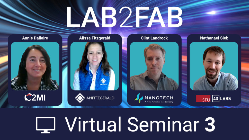
Virtual Seminar 3
Welcome – Opening remarks
Moderator:
Annie Dallaire
MSc MBA Vice-President, Business development
C2MI
Description:
When to move from a development lab into a foundry and the timeline and tasks (and money!) required for successful foundry transfer.
 Alissa M. Fitzgerald, Ph.D.
Founder & CEO, A.M. Fitzgerald & Associates, LLC
Description:
4D LABS is an open-access applications- and science-driven Core Facility at Simon Fraser University in BC. It provides a wide range of capabilities to academic and industrial researchers to fabricate and characterize the next generation of advanced materials and devices.

Nathanael Sieb
Director of Operations and Administration
4D LABS, Simon Fraser University
Nathanael Sieb is the Director of Operations and Administration at 4D LABS, an open-access Nanofabrication and Characterization facility at Simon Fraser University. He is responsible for day-to-day operations, business development, and long-term sustainability planning for the facility.
Over the last fifteen years he has worked in the nanofabrication and advanced characterization field in a variety of roles. As a researcher he worked on developing new techniques for the self-assembly of materials, as a technician he was responsible for training and maintenance on a diverse set of fabrication tools, and as a director he is responsible for an open-access facility serving the needs of over 140 companies and 1200 researchers.
4D LABS is a $75mil core facility at Simon Fraser University focused on advanced materials research. It officially opened in 2010 and since then it has continued to attract researchers and funding and it has been critical to the rapid growth of the BC Tech sector. Through multiple grants 4D LABS has continued to grow and now offers over 100 tools throughout its 30,000 sq-ft facility. Research in the facility spans multiple disciplines including clean tech, life science, MEMS, and more.
Nathanael Sieb received his B.Sc. in Chemical Physics in 2005 and his M.Sc. in Chemistry in 2008 from Simon Fraser University.
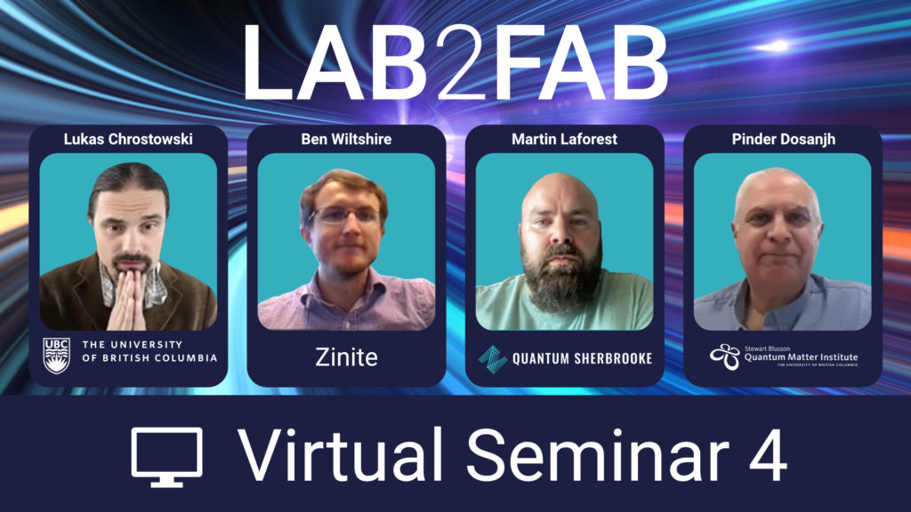
Virtual Seminar 4
Welcome – Opening remarks
Moderator:

Lukas Chrostowski, PhD
Professor of Electrical and Computer Engineering
University of British Columbia
Description:
The presentation will cover how Zinite is pioneering the new frontier of Moore’s Law and how Canada can participate at the leading edge – a perspective from the front lines of R&D.

Ben Wiltshire
Modeling & Test Senior Engineer
Zinite
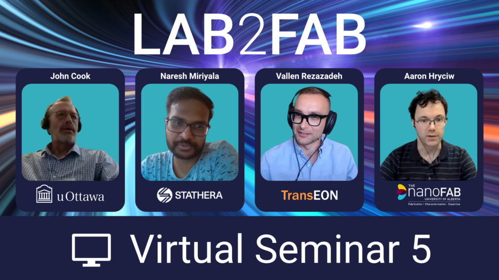
Virtual Seminar 5
Welcome – Opening remarks
Moderator:
John Cook
Description:
Despite deep talent and research capacity, the Canadian semiconductor industry has remained small in size and impact compared to our peers in Europe and Asia. This presentation will explore factors at play and how to position ourselves for future success.

Vallen Rezazadeh
Founder and CEO
TransEON Inc.

Aaron Hryciw, PhD, PEng
Fabrication Group Manager
University of Alberta – nanoFAB
Aaron Hryciw is the Fabrication Group Manager at the University of Alberta nanoFAB Centre, a national, open-access training, service, and collaboration centre, focused on academic and industrial applications in micro- and nanoscale fabrication and characterization. Totalling over $100M in specialized equipment and infrastructure, with over 200 pieces of equipment in 25 000 sq ft of communal laboratory space, the nanoFAB hosts complete capabilities for microscopy, spectroscopy, material analysis, lithography, thin-film deposition, and etching.
After receiving a BSc in Engineering Physics and a PhD in Physics from the University of Alberta, Aaron cut his nanofabrication teeth as a postdoctoral fellow at Stanford University. Returning to Edmonton, he worked as a research associate at the National Institute for Nanotechnology, designing and fabricating nanophotonic devices for optomechanical sensing and quantum information processing. At the nanoFAB, Aaron coordinates and oversees all activities of the fabrication group, including fee-for-service projects, collaborations, and user training.
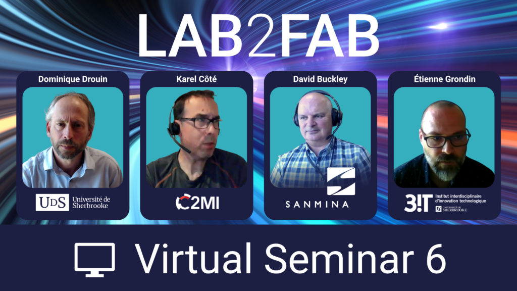
Virtual Seminar 6
Welcome – Opening remarks
Moderator:

Dominique Drouin, PhD EIT

Karel Côté, M.Sc.
Senior Microfabrication Technical Specialist
C2MI
Karel Côté obtained a Physics degree at University of Sherbrooke (1997) and a master’s degree in biophysics/physiology at University of Sherbrooke (2000). He then joined Mitel Semiconductor Bromont, Qc, Canada plant (that would become Teledyne DALSA) as a photolithography scientist specializing in process/masks integration, 2D/3Dmetrology, and alignment/exposure until 2014. During this time, Teledyne-DALSA went from CMOS/CCD microfabrication to almost uniquely MEMS fabrication using legacy CMOS tool. He then joined the NRC of Canada (Boucherville, Qc) as a microfabrication specialist for printable electronics and Biochips for 2 years.
In 2016, Karel finally joined the MiQro Innovation Collaborative Center [C2MI] as a microfabrication specialist where he develops multitude of specialized MEMS process and helps with his wide background in the rapid growth of this young “one-of-a-kind” development center.
Karel is part of the technical specialist team of the CII (Integrated Innovation chain) connecting C2MI with 3IT (Interdisciplinary Institute for Technological Innovation) and the IQ (Quantum Institute), establishing a relationship from Research, early prototyping to industrialisation of microfabrication processes).
Description:
The integration of compound semiconductors, silicon photonics and advanced ASICS is required for critical, next generation applications.
At Sanmina’s Advanced Microsystems Technologies, our engineering of innovative solutions, combined with our advanced manufacturing environment, enables your path to market.

David Buckley
VP, Development Engineering
Sanmina, Advanced Microsystems Technologies Division


Étienne Grondin
Laboratory Manager
3iT (UdS) nanofabrication facility
Mr. Grondin joined the Université de Sherbrooke as a research engineer in 2003 and has held the position of nanofabrication infrastructure manager since 2009. He is now in charge of a team of 20 employees and has acquired a broad experience in everything related to the management and operation of a large research infrastructure. He has been actively involved in the development of the 3iT and the shared technological platform models at UdS. He is also a key member of the Integrated Innovation Chain formed by the UdS Quantum Institute, 3iT and C2MI.
Mr. Grondin obtained his B.Sc in Engineering Physics in 2003 and his M.Sc degree in Electrical Engineering in 2005 from Université Laval. He co-founded the start-up company SWAG Technologies in 2001. He is co-author of 5 patents and several scientific publications. His technical and scientific expertise mainly relates to simulation and fabrication of microelectronic, photonic and quantum devices.
 Ayse Turak
Director of the Centre for Emerging Device Technologies
McMaster University
Ayse Turak is an Associate Professor in the Department of Engineering Physics and Director of the Centre for Emerging Device Technologies, at McMaster University. Her research focusses on growth of organic and hybrid organic-inorganic (perovskite) thin films and nanoparticles for microelectronics. Her vision is to develop easy, versatile, and inexpensive methods of exploring and tuning interfaces, targeting energy applications, sensing and magneto-optics. By making electronic products cheaper, more accessible, and more flexible, her research will have a huge impact on the way people use clean energy, access information and measure the world around them. She is an associate member of the Department of Materials Science and Engineering and the School of Biomedical Engineering at McMaster.
Prior to McMaster, she was a Marie Curie Fellow at the Max-Planck-Institute for Metals Research (Germany, 2008-2010), then a visiting professor at Sabanci University (Turkey, 2011). She has received an Early Researcher Award (2016), a Leadership in Teaching and Learning Fellowship (2017-2019) and the Petro-Canada Young Innovators award (2016). In the international research community, she serves as the co-chair for the Canadian chapter for the Society for Information Display, the director of the Functional Materials Research Consortium (with Hoseo University and A-Pro Ltd, S. Korea), and as a member of the Canadian Printable Electronics Industry Association/intelliFLEX Innovation Alliance, and EVATEG (Energy Efficient Electronic and Lighting Technologies Research Centre, Turkey). She also sits on the Editorial Board for the Journal of Materials Science: Materials in Electronics (Springer) and Scientific Reports (Springer-Nature), and as Associate editor for Frontiers in Photonics in Photovoltaic Materials and Devices.
As a member of multiple equity seeking groups, she champions colleagues and students from under-represented communities, and celebrates their success, through her service in a variety of roles. She integrates equity, diversity, inclusion and accessibility in her teaching philosophy to achieve excellence in the pedagogy of science.
Who Benefits from LAB2FAB?
- Academic-based fabrication and characterization centres
- Government laboratories
- Manufacturers and supply chain
- Technology developers
- Company builders
- Stakeholders in collaborative innovation
