LAB2FAB
Workshop 2022
Shedding Light on Innovation
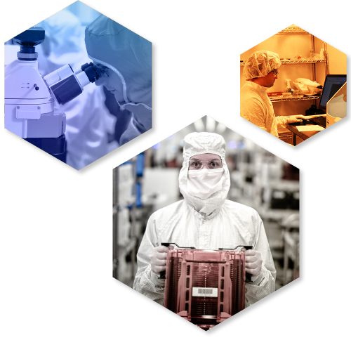
Micro-nanotechnology facilities at Canadian universities are a national asset for helping innovators advance and manage their R&D activities. The LAB2FAB bi-annual meeting provides a platform for industry, academic-based fabrication and characterization centres, and government labs to collaborate in overcoming their R&D challenges.
Our goal is to help all parties build their capacity and expertise to increase Canadian competitiveness in manufacturing of microsystems and nanotechnology innovations through team efforts to:
- Enhance connections among technology developers to maximize benefit from technology offerings throughout the Canadian ecosystem.
- Enhance access to infrastructure inside Canada and exchange value in cross-border partnerships.
- Connect funding opportunities to technology resources and end users.
- To encourage rich exchange among all participants, every speaker session also dedicates time for plenary discussion.
Register for Virtual Seminars (No Fee)
Virtual Seminar 1
Welcome – Opening remarks
Moderator:
CMC Microsystems
Gord Harling
President and CEO, CMC Microsystems
Gordon Harling received a Bachelor’s degree in Applied Science from the University of Toronto and a Maîtrise en Ingénierie Physique from Polytechnique Montréal. He has worked in Research and Development at large companies such as Mitel, NovAtel, and DALSA. He has been a founder and CEO of several start-up companies including Goal Semiconductor, Elliptic Technologies, and Innotime Technologies. He joined CMC Microsystems in February 2018 as President and CEO.
Mohsen K. Akhlaghi
Director of Integrated Photonics, Photonic Inc.
Mohsen K. Akhlaghi received his B.Sc. and M.Sc. in electrical engineering from Tehran Polytechnic in 2000 and 2003. He held a variety of engineering and management positions in the industrial and consumer electronics sector. His Ph.D. from the University of Waterloo in 2012 was on detecting single photons using superconducting nanowires. After a postdoctoral at UBC, he joined Nanotech Security Corp. later acquired by Meta Materials Inc. Mohsen is currently Director of Integrated Photonics at Photonic Inc
Virtual Seminar 2
Description:
Discover the making of AEPONYX’s technology leadership through numerous academic and industrial collaborations, leading to the creation of an advanced photonics integrated circuit platform. Learn about the Silicon Nitride with MEMS circuits and the complete optical packaging capabilities from AEPONYX.
Philippe Babin
CEO, AEPONYX Inc.
Lukas Chrostowski, PhD
Professor of Electrical and Computer Engineering,
University of British Columbia
Lukas Chrostowski is a Professor of Electrical and Computer Engineering at the University of British Columbia, Vancouver, BC, Canada. Born in Poland, he earned the B.Eng. in electrical engineering from McGill University and the PhD in electrical engineering and computer science from the University of California at Berkeley. With research interests in silicon photonics, optoelectronics, high-speed laser (VCSEL) design, fabrication and test, for applications in optical communication systems and biophotonics, he has published more than 200 journal and conference publications. He co-edited a book “High-Speed Photonics Interconnects” (2013), and co-authored the book “Silicon Photonics Design” (Cambridge University Press, 2015). Dr. Chrostowski served as the co-director of the University of British Columbia AMPEL Nanofabrication Facility (2008-2017). He is the Program Director the NSERC CREATE Silicon Electronic-Photonic Integrated Circuits (Si-EPIC) research training program in Canada, and has been teaching numerous silicon photonics workshops and courses since 2008. He spent his 2011-12 sabbatical at the University of Washington, Seattle, with Michael Hochberg’s group. Chrostowski received the Killam Teaching Prize at the University of British Columbia in 2014. He was an elected member of the IEEE Photonics 2014-2016 Society Board of Governors and serves as the Associate VP of Education (2014-). He was awarded a Natural Sciences and Engineering Research Council of Canada Discovery Accelerator Supplements Award in 2015.
Dr. Pierre Berini
University of Ottawa NanoFab
Pierre Berini (F’11) received his Ph.D. and M.Sc.A. degrees in Electrical Engineering from École Polytechnique de Montréal, Canada, and his B.E.Sc. and B.Sc. degrees in Electrical Engineering and Computer Science, respectively, from the University of Western Ontario, Canada. Dr. Berini is Distinguished University Professor of Electrical Engineering and of Physics, University Research Chair in Surface Plasmon Photonics, former Director of the Centre for Research in Photonics at the University of Ottawa, and Director of the uOttawa Nanofab. He was the Founder and Chief Technology Officer of a venture capital financed company and he collaborates on an ongoing basis with industry.
Dr. Berini has received an NSERC Steacie Fellowship, an NSERC Discovery Accelerator, a Premier of Ontario Research Excellence Award (PREA), the University of Ottawa Young Researcher of the Year Award, an URSI Young Scientist Award, a George S. Glinski Award for Excellence in Research, and is a Canada Foundation for Innovation researcher. Dr. Berini is a Fellow of the IEEE, a Fellow of the OSA, a Fellow of the APS, a Fellow of the Canadian Academy of Engineering, and a Fellow of the Royal Society of Canada. He has published 12 book chapters, approximately 600 scientific and technical papers in peer-reviewed periodicals and conference proceedings (h = 51), and is an inventor or co-inventor on 24 patents. He was an Associate Editor of Optics Express and a Managing Editor of Nanophotonics, and is presently an Associate Editor of Optica. He contributes on an ongoing basis to the organization of several international conferences in photonics. His research interests span many areas of optics and photonics, with surface plasmons, metasurfaces and their applications being of present interest.
Virtual Seminar 3
Welcome – Opening remarks
Moderator:
Annie Dallaire
MSc MBA Vice-President, Business development
C2MI
Description:
When to move from a development lab into a foundry and the timeline and tasks (and money!) required for successful foundry transfer.
Alissa M. Fitzgerald, Ph.D.
Founder & CEO, A.M. Fitzgerald & Associates, LLC
Description:
4D LABS is an open-access applications- and science-driven Core Facility at Simon Fraser University in BC. It provides a wide range of capabilities to academic and industrial researchers to fabricate and characterize the next generation of advanced materials and devices.
Nathanael Sieb
Director of Operations and Administration
4D LABS, Simon Fraser University
Nathanael Sieb is the Director of Operations and Administration at 4D LABS, an open-access Nanofabrication and Characterization facility at Simon Fraser University. He is responsible for day-to-day operations, business development, and long-term sustainability planning for the facility.
Over the last fifteen years he has worked in the nanofabrication and advanced characterization field in a variety of roles. As a researcher he worked on developing new techniques for the self-assembly of materials, as a technician he was responsible for training and maintenance on a diverse set of fabrication tools, and as a director he is responsible for an open-access facility serving the needs of over 140 companies and 1200 researchers.
4D LABS is a $75mil core facility at Simon Fraser University focused on advanced materials research. It officially opened in 2010 and since then it has continued to attract researchers and funding and it has been critical to the rapid growth of the BC Tech sector. Through multiple grants 4D LABS has continued to grow and now offers over 100 tools throughout its 30,000 sq-ft facility. Research in the facility spans multiple disciplines including clean tech, life science, MEMS, and more.
Nathanael Sieb received his B.Sc. in Chemical Physics in 2005 and his M.Sc. in Chemistry in 2008 from Simon Fraser University.
Virtual Seminar 4
Welcome – Opening remarks
Moderator:
Lukas Chrostowski, PhD
Professor of Electrical and Computer Engineering
University of British Columbia
Virtual Seminar 5
Welcome – Opening remarks
Moderator:
Karin Hinzer, MSc PhD
Vice-Dean, Research of the Faculty of Engineering and Professor
University of Ottawa
Aaron Hryciw, PhD, PEng
Fabrication Group Manager
University of Alberta – nanoFAB
Aaron Hryciw is the Fabrication Group Manager at the University of Alberta nanoFAB Centre, a national, open-access training, service, and collaboration centre, focused on academic and industrial applications in micro- and nanoscale fabrication and characterization. Totalling over $100M in specialized equipment and infrastructure, with over 200 pieces of equipment in 25 000 sq ft of communal laboratory space, the nanoFAB hosts complete capabilities for microscopy, spectroscopy, material analysis, lithography, thin-film deposition, and etching.
After receiving a BSc in Engineering Physics and a PhD in Physics from the University of Alberta, Aaron cut his nanofabrication teeth as a postdoctoral fellow at Stanford University. Returning to Edmonton, he worked as a research associate at the National Institute for Nanotechnology, designing and fabricating nanophotonic devices for optomechanical sensing and quantum information processing. At the nanoFAB, Aaron coordinates and oversees all activities of the fabrication group, including fee-for-service projects, collaborations, and user training.
Day 1 - September 25
Evening
Registration | Networking
19:00 – 21:00
TBC
Welcome Reception
Day 2 - September 26
08:45 – 09:00
Welcome
09:00 – 10:00
Session 1: Lab of the future
Innovations in the usage and management of nanofabrication labs.
- What noteworthy processing capabilities are emerging in open-access facilities?
- What expertise and services are users looking for in facilities?
- What do success stories teach us about the most promising R&D opportunities that can benefit from laboratory capabilities?
10:30 – 11:00
Networking Break
11:00 – 12:30
Session 2: Bridging discovery to production
Positioning technology development for commercialization and scale-up.
- Success stories of climbing the TRL ladder, technology transfer, and scale up.

Alissa M. Fitzgerald
Founder & CEO
A.M. Fitzgerald & Associates, LLC

Chiara Alessandri
Luceda Photonics
12:30 – 13:30
Networking Lunch
13:30 – 14:50
Session 3: R&D Milestones and Future Talent
- Share company vision, technology goals, and R&D milestones.
- What skills are needed in tomorrow’s microsystems workforce?
- Connect with Rising Stars for follow-up networking.

Ben Wiltshire
Modeling & Test Senior Engineer
Zinite

Clint Landrock
Vice President, Technology & Innovation
Nanotech
14:50 – 15:20
Networking Break
15:20 – 16:20
MNT Labs Cataloging and Roadmap Session
16:20 – 18:00
Adjourn
18:00 – 20:00
Dinner Reception
Day 3 - September 27
08:30 – 09:00
Welcome
09:00 – 10:45
Session 4: Photonic Integrated Circuits – A Flourishing Canadian Ecosystem
An ecosystem view of the silicon photonics value chain in Canada.
- Examples of advancing photonics developments from concept to product.
- Connect to a network initiative or proposal.
- Understand industry needs in business and process capability.
10:45 – 11:15
Networking Break
11:15 – 12:15
Session 5: Taking the Next Steps Together
- What megatrends that will shape the next 10 years? Where should R&D efforts focus?
- What have the last two years taught us about the possibilities of a better normal?
- What actions should be taken after this workshop to pursue specific opportunities?
- And more…
12:15 – 12:30
Adjourn workshop
12:30 – 13:30
Networking Lunch
Who Benefits from LAB2FAB?
- Academic-based fabrication and characterization centres
- Government laboratories
- Manufacturers and supply chain
- Technology developers
- Company builders
- Stakeholders in collaborative innovation